


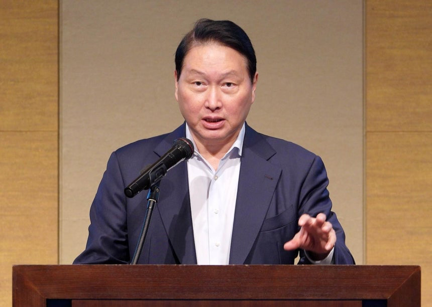
- Chairman Chey Tae-won at the Sendai Korea-Japan Chamber of Commerce Meeting on the 31st: "Considering Everywhere with Good Water and Power"
- Miyagi Prefecture Uses 300,000㎡ Site for Sub-surface Love Call… Targeting Kumamoto-style Boom Driven by TSMC
- CEO Kwak Noh-jung Says "Hopes to Contribute to Japan's Semiconductor Industry"… US Commerce Secretary's Domestic Investment Pressure is a Key Variable
- Experts Say "A Mid-to-Long-Term Strategy to Secure Global Memory Market Leadership Through Proactive Investment 2-3 Years Ahead"
SK Group has officially raised the possibility of building a new semiconductor plant (fab) in Japan. Amid intensifying inter-state competition for global semiconductor hegemony, the Japanese government and local authorities have jumped into the battle to win over SK Hynix, backed by unprecedented infrastructure incentives.
SK Group Chairman Chey Tae-won met with reporters right after the 15th Korea-Japan Chamber of Commerce and Industry Chairman Meeting held in Sendai, Miyagi Prefecture, Japan, on the 31st (local time). When asked about the possibility of building a fab in Japan, he stated, "We are currently in the review process. We will let you know as soon as the review is complete." Regarding favorable location conditions, he said, "We are looking all over Japan," adding, "We can look anywhere with good power and water." Bloomberg reported that establishing a joint venture with a local company or pursuing a small-scale acquisition are being discussed as likely options.
Japanese local governments immediately entered the competition to attract the fab. According to reports by the Nihon Keizai Shimbun, Miyagi Prefecture has proposed a 300,000㎡ site within the 'Second Sendai Northern Core Industrial Park' in Ohira-mura near Sendai to SK Hynix and is conducting behind-the-scenes negotiations. The region emphasizes its geographic advantages—being clustered with Tohoku University researchers and major production bases of semiconductor equipment maker Tokyo Electron—along with abundant water and power infrastructure. The strategy is to replicate the success of Kumamoto Prefecture, which reaped massive economic ripple effects by attracting a TSMC plant. SK Hynix has also indirectly held stakes in Japanese NAND flash company Kioxia and increased exchanges with local material and equipment companies.
However, explicit pressure from the US to invest domestically remains a major variable in determining the fab's location. US Commerce Secretary Howard Lutnick recently targeted Micron's competitors, raising the pressure by stating, "Samsung Electronics and SK Hynix also want to produce in the US."
Regarding this, SK Hynix CEO Kwak Noh-jung recently remarked at the groundbreaking ceremony for the advanced packaging fab in Indiana, USA, "Just as we contribute to the AI industry in the US, we also want to contribute to Japan's semiconductor business," adding, "We are carefully reviewing how to develop the NAND flash market together with customers and partners." Distancing himself from expanded US investment, Kwak noted, "If there are places that provide sufficient resources like water, power, talent, and subsidies, (semiconductors) are open to being built anywhere," but added, "Since nothing has been finalized yet, we cannot discuss details or direction."
Experts interpret this diversification of production bases as a strategy to solidify market dominance. Lee Jong-hwan, a professor of system semiconductor engineering at Sangmyung University, diagnosed, "The reason SK Hynix is considering investments in Yongin, Honam, the US, and Japan is because it judges that there are opportunities to leap forward in the memory market. Since semiconductors are an industry where investment effects take two to three years to materialize, this appears to be a strategy to secure production capacity through preemptive investment and pioneer the global market."